Production Capacity :- 5000 sqm / month Sector Catered : Automotive, Lighting, Industrial Electronics, Home Appliances, Railways, Power Electronics, Automation, Storage Devices, Solar Systems & EV.
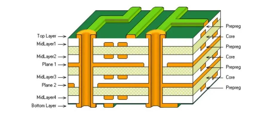
What is Multilayer PCB
A multilayer PCB is a type of printed circuit board that consists of multiple layers of conductive material separated by insulating layers. These layers are laminated together under high pressure and temperature to create a single, unified board. Multilayer PCB typically have four or more layers, including two outer layers and one or more inner layers.
Pros of Multilayer PCB
Higher Component Density: Multilayer PCB allow for a higher density of components in a smaller footprint, making them ideal for complex and compact electronic devices.
Improved Performance: The additional layers enable more intricate and efficient routing of electrical signals, leading to improved performance, reduced signal interference, and lower crosstalk.
Enhanced Design Flexibility: Designers have more flexibility to place components and route signals, which is beneficial for sophisticated and high-speed circuits.
Increased Functionality: The ability to add more layers allows for the integration of more functions and features within a single board, supporting advanced applications.
Thermal Management: Multilayer PCB can incorporate thermal vias and heat dissipation layers to better manage and distribute heat, which is crucial for high-power applications.
Durability and Reliability: The lamination process and the use of multiple layers enhance the mechanical strength and reliability of the PCB, making it more durable.
Cons of Multilayer PCB
Higher Component Density: Multilayer PCB allow for a higher density of components in a smaller footprint, making them ideal for complex and compact electronic devices.
Improved Performance: The additional layers enable more intricate and efficient routing of electrical signals, leading to improved performance, reduced signal interference, and lower crosstalk.
Enhanced Design Flexibility: Designers have more flexibility to place components and route signals, which is beneficial for sophisticated and high-speed circuits.
Increased Functionality: The ability to add more layers allows for the integration of more functions and features within a single board, supporting advanced applications.
Thermal Management: Multilayer PCB can incorporate thermal vias and heat dissipation layers to better manage and distribute heat, which is crucial for high-power applications.
Durability and Reliability: The lamination process and the use of multiple layers enhance the mechanical strength and reliability of the PCB, making it more durable.
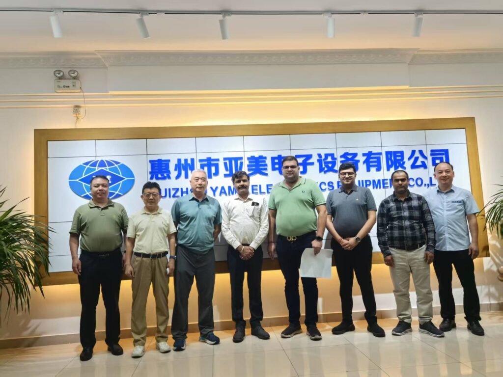
In a strategic move to strengthen our manufacturing capabilities and adopt cutting-edge technology, Team Signum recently completed a successful visit to China to explore and procure state-of-the-art equipment for our upcoming PCB production unit in Jammu.
The visit was part of our continuous commitment to innovation and excellence in the PCB industry. During the tour, our senior technical and operations team engaged with leading global manufacturers of PCB machinery and automation systems. The objective was to identify and integrate next-generation equipment that would enhance production efficiency, quality control, and scalability at our new facility.
Nov 11, 2024
Signum has successfully completed an audit with KIA Motors on 06-11-2024
May 28, 2025
A POSH (Prevention of Sexual Harassment) training awareness session was successfully conducted at Signum by an external trainer, Ms. Malvika.
In a strategic move to strengthen our manufacturing capabilities and adopt cutting-edge technology, Team Signum recently completed a successful visit to China to explore and procure state-of-the-art equipment for our upcoming PCB production unit in Jammu.
The visit was part of our continuous commitment to innovation and excellence in the PCB industry. During the tour, our senior technical and operations team engaged with leading global manufacturers of PCB machinery and automation systems. The objective was to identify and integrate next-generation equipment that would enhance production efficiency, quality control, and scalability at our new facility.
Team Signum Visits China to Upgrade Equipment for Advanced PCB Production at New Jammu Facility
In a strategic move to strengthen our manufacturing capabilities and adopt cutting-edge technology, Team Signum recently completed a successful visit to China to explore and procure state-of-the-art equipment for our upcoming PCB production unit in Jammu.
The visit was part of our continuous commitment to innovation and excellence in the PCB industry. During the tour, our senior technical and operations team engaged with leading global manufacturers of PCB machinery and automation systems. The objective was to identify and integrate next-generation equipment that would enhance production efficiency, quality control, and scalability at our new facility.