Design and Prototyping : The journey begins with a comprehensive PCB design. Using advanced CAD tools, our design team works closely with clients to create custom layouts based on specific project requirements.
PCB Material Selection : Choosing the right materials is critical to ensure performance and durability. Depending on the project needs, we select from a range of high-quality materials such as FR4.
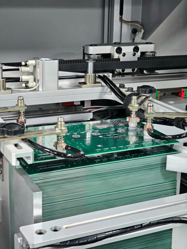
Cutting and Drilling : Next, drilling of vias (small holes) is performed to create electrical connections between layers. These drilled holes are then plated with copper to ensure proper conductivity between layers.
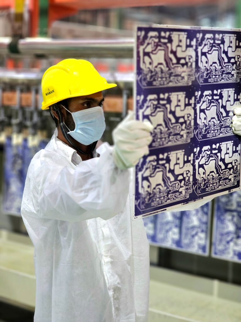
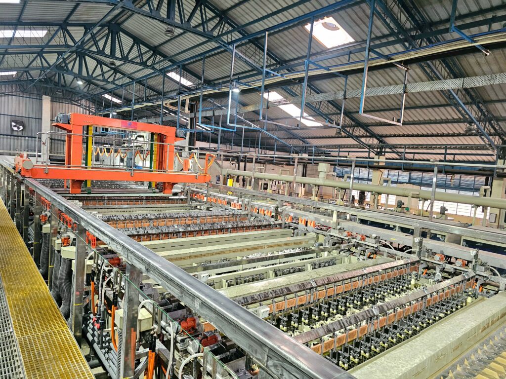
Photolithography & Plating : Photolithography is a precise and widely used technique in the semiconductor and microfabrication industries to pattern designs on substrates. This process plays a pivotal role in creating printed circuit boards (PCB).
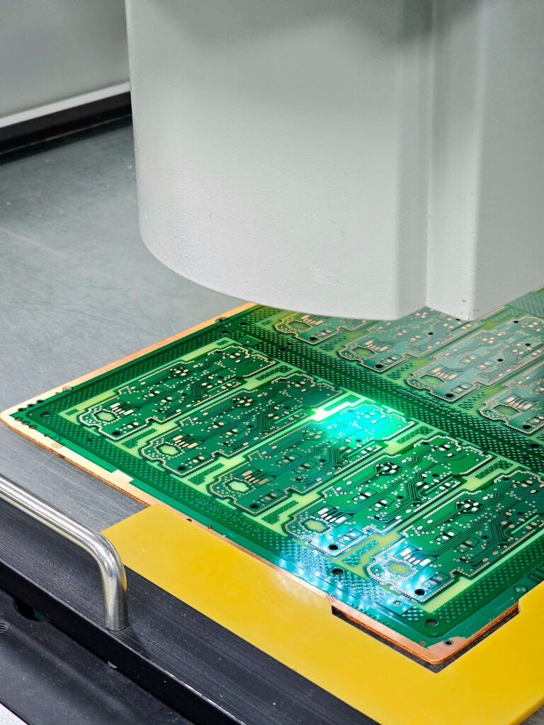
Micro Section & Etching : Micro-sectioning and Automated Optical Inspection (AOI) are critical post-etching quality control steps in PCB (Printed Circuit Board) manufacturing & checked different defects like PTH thickness, Line width violations, spacing violations, excess copper, short or open circuits, etc.
Solder Mask and Developing : A solder mask is applied over the etched copper surface of a printed circuit board (PCB) to protect it from environmental contaminants and oxidation. This protective layer also helps define the areas where components will be soldered by preventing solder bridges between closely spaced pads.
Surface Finish :Lead-Free HASL, OSP, Immersion Gold, and Immersion Tin are common PCB surface finishes, each with unique properties and applications.
Quality Testing : To ensure and validate product quality, various tests are performed, including Electrical Testing, Solderability Testing, Hole Checking, Automated Visual Inspection (AVI), and profile verification using a (VMS)
Packaging and Delivery : The final product is vacuum-packed with silica dioxide and securely enclosed in robust corrugated boxes to safeguard against environmental factors. We ensure safe packaging and collaborate with trusted shipping partners to guarantee timely and secure delivery to your location.
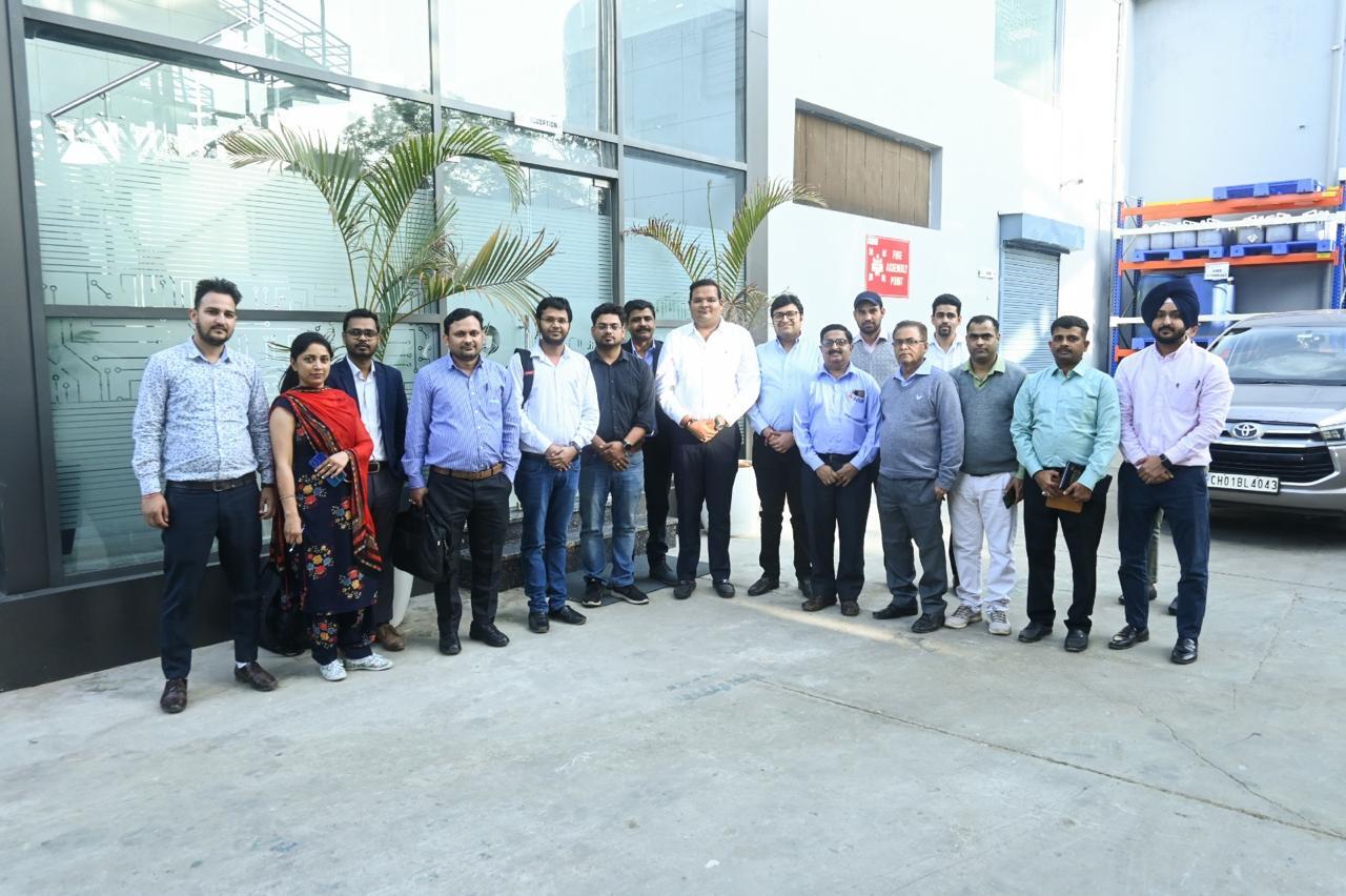
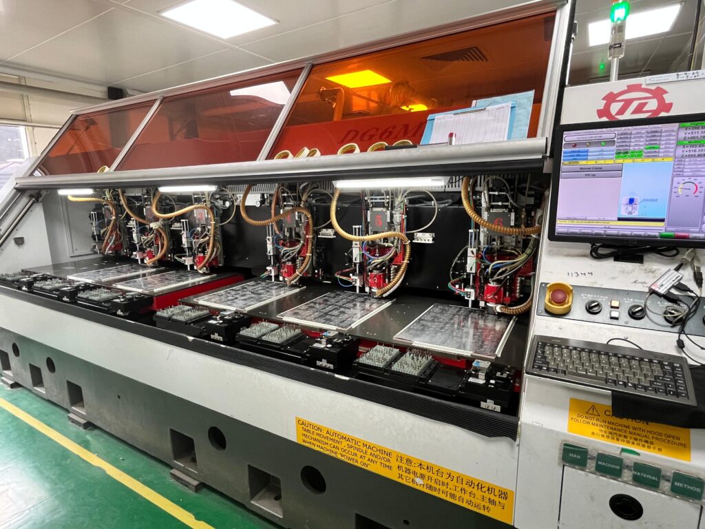
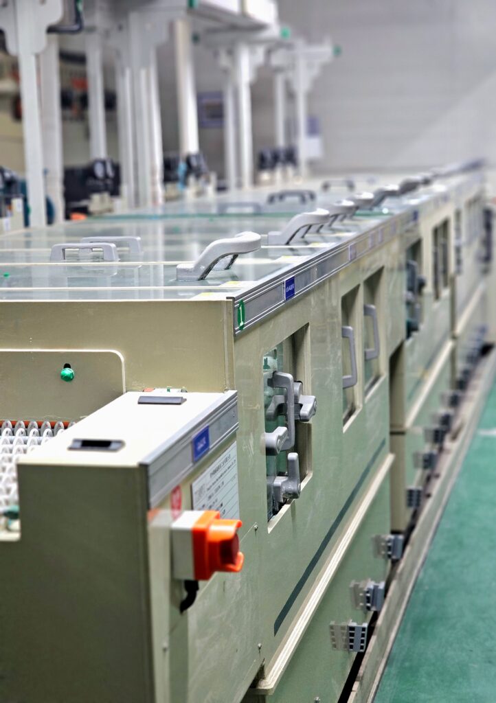
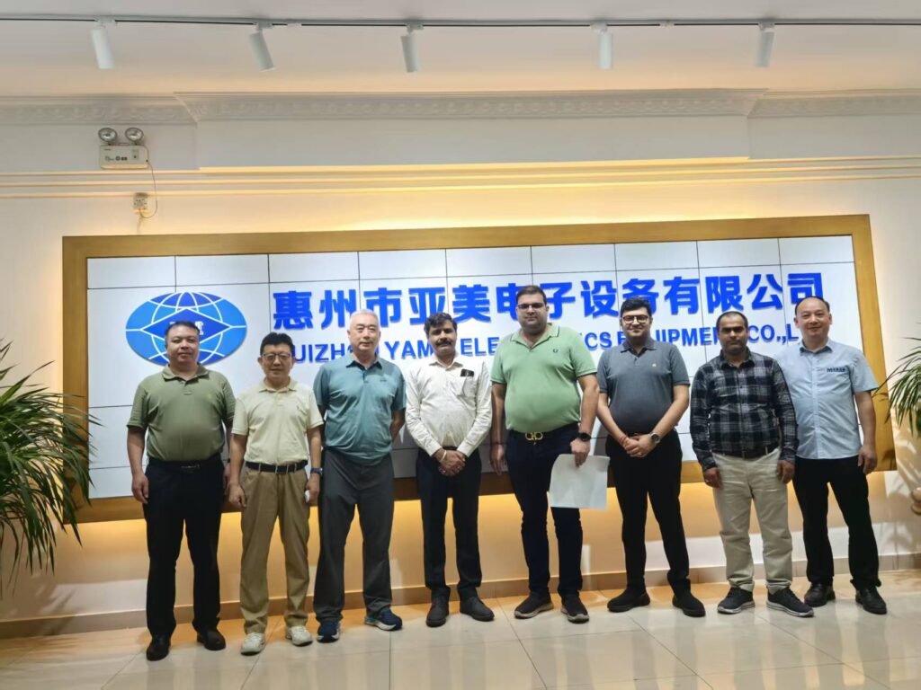
In a strategic move to strengthen our manufacturing capabilities and adopt cutting-edge technology, Team Signum recently completed a successful visit to China to explore and procure state-of-the-art equipment for our upcoming PCB production unit in Jammu.
The visit was part of our continuous commitment to innovation and excellence in the PCB industry. During the tour, our senior technical and operations team engaged with leading global manufacturers of PCB machinery and automation systems. The objective was to identify and integrate next-generation equipment that would enhance production efficiency, quality control, and scalability at our new facility.
Nov 11, 2024
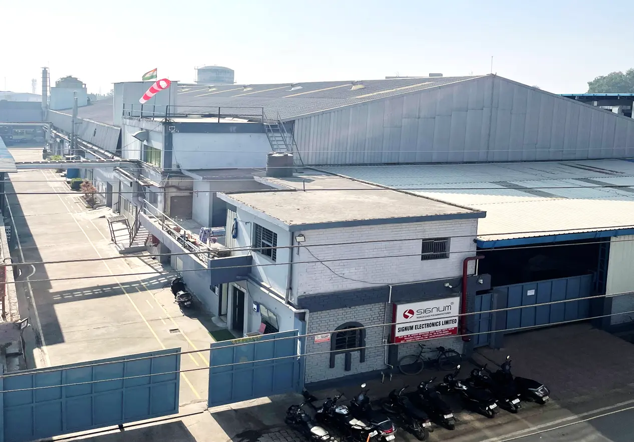
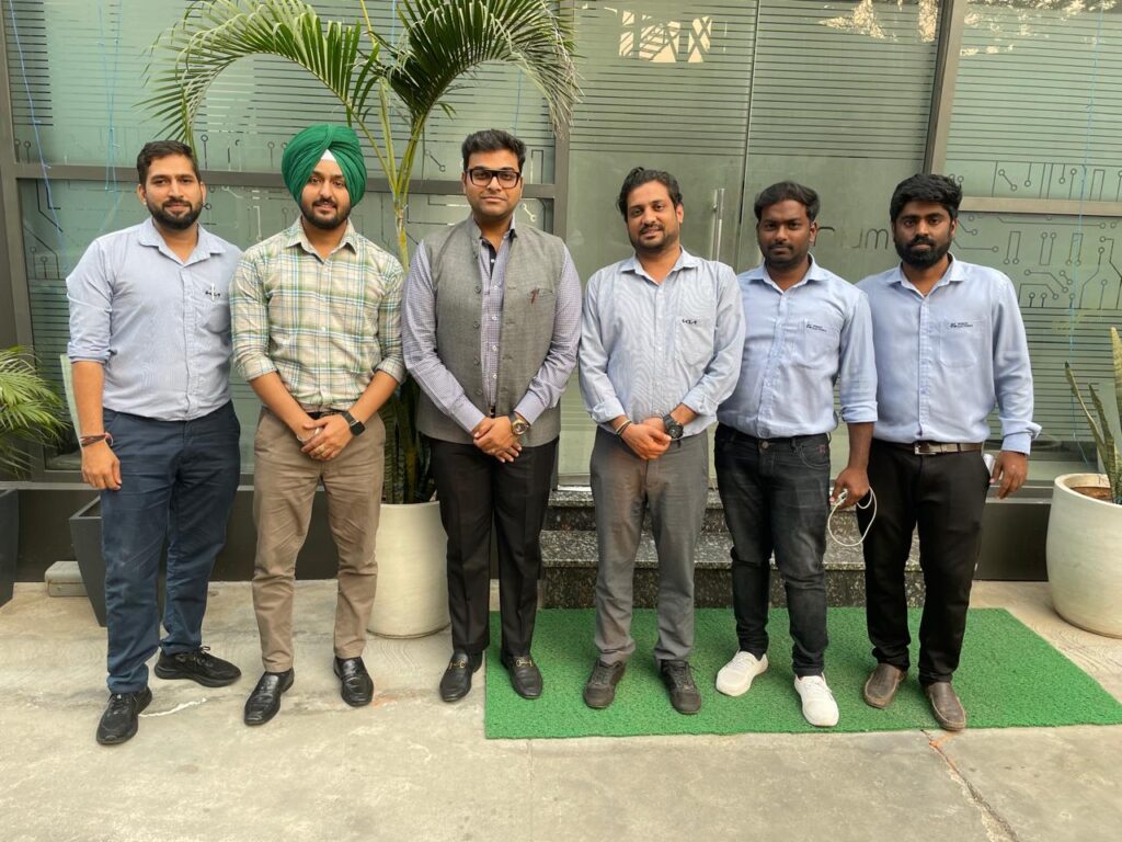
Signum has successfully completed an audit with KIA Motors on 06-11-2024
May 28, 2025
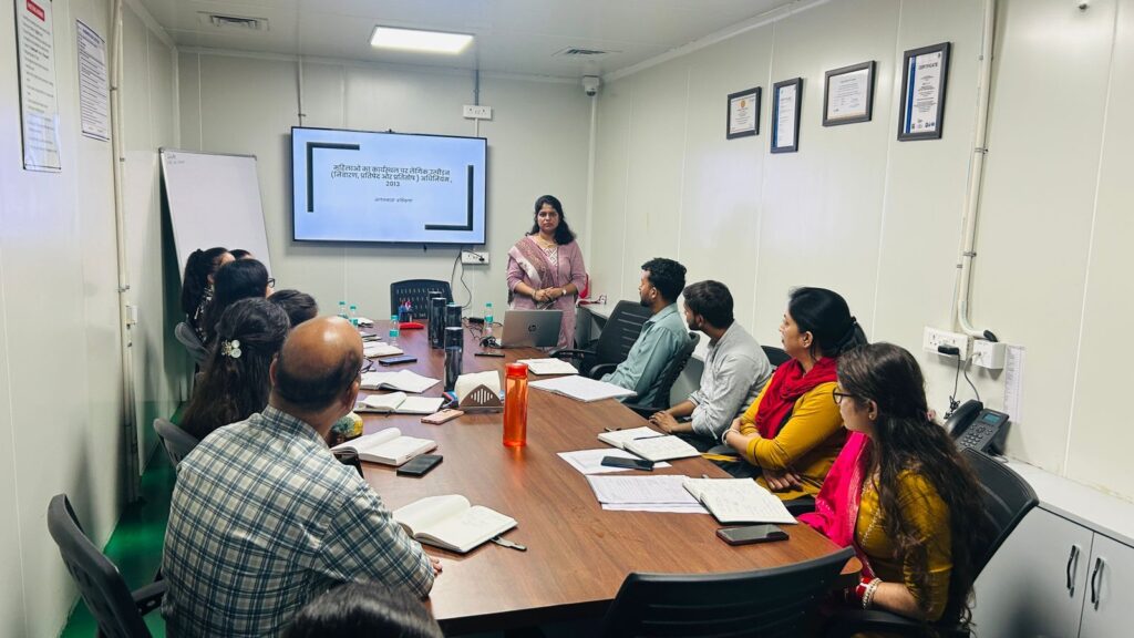
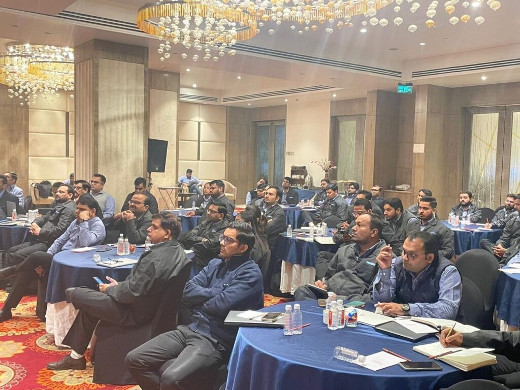
A POSH (Prevention of Sexual Harassment) training awareness session was successfully conducted at Signum by an external trainer, Ms. Malvika.
In a strategic move to strengthen our manufacturing capabilities and adopt cutting-edge technology, Team Signum recently completed a successful visit to China to explore and procure state-of-the-art equipment for our upcoming PCB production unit in Jammu.
The visit was part of our continuous commitment to innovation and excellence in the PCB industry. During the tour, our senior technical and operations team engaged with leading global manufacturers of PCB machinery and automation systems. The objective was to identify and integrate next-generation equipment that would enhance production efficiency, quality control, and scalability at our new facility.
Team Signum Visits China to Upgrade Equipment for Advanced PCB Production at New Jammu Facility
In a strategic move to strengthen our manufacturing capabilities and adopt cutting-edge technology, Team Signum recently completed a successful visit to China to explore and procure state-of-the-art equipment for our upcoming PCB production unit in Jammu.
The visit was part of our continuous commitment to innovation and excellence in the PCB industry. During the tour, our senior technical and operations team engaged with leading global manufacturers of PCB machinery and automation systems. The objective was to identify and integrate next-generation equipment that would enhance production efficiency, quality control, and scalability at our new facility.