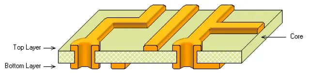
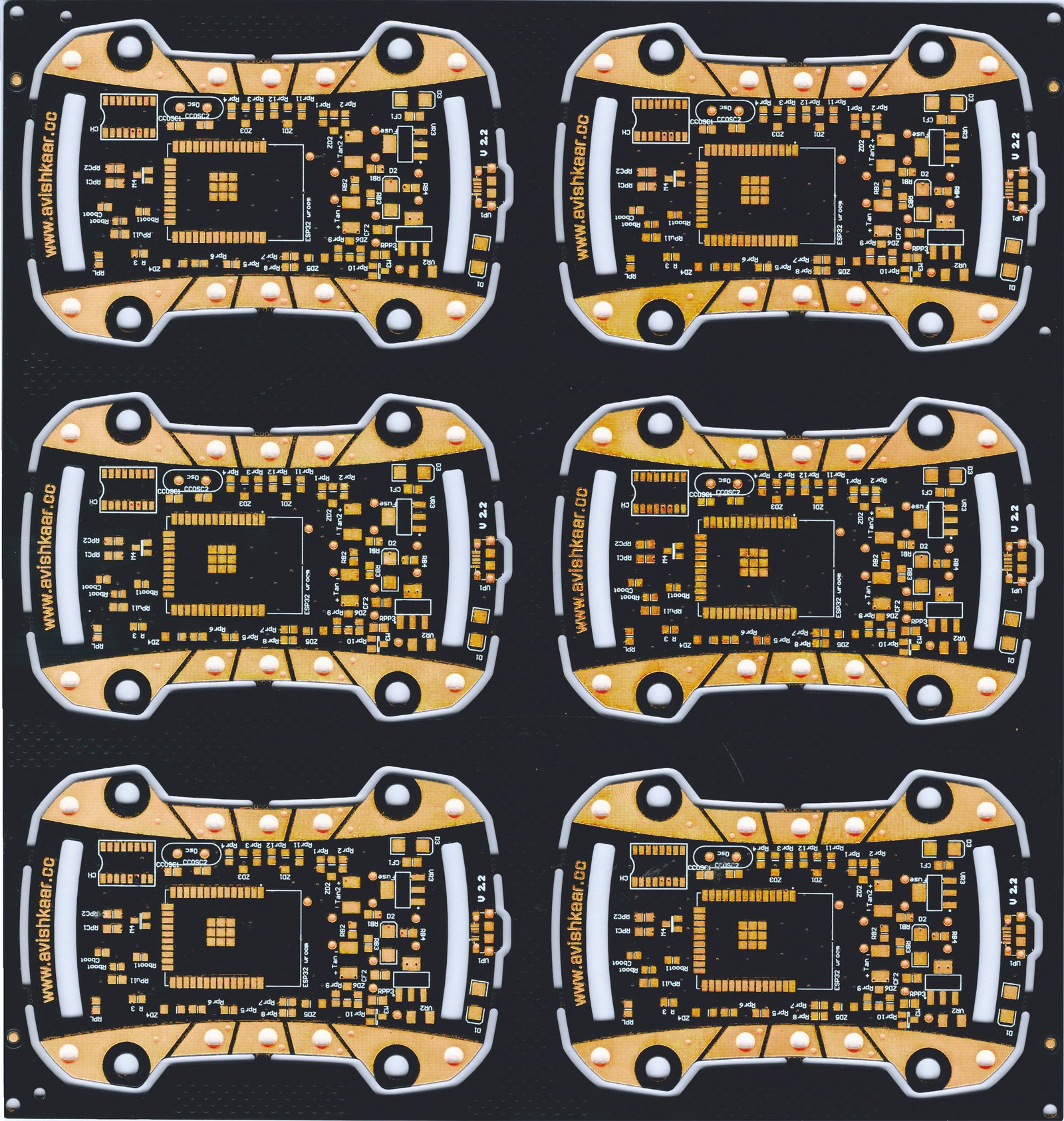
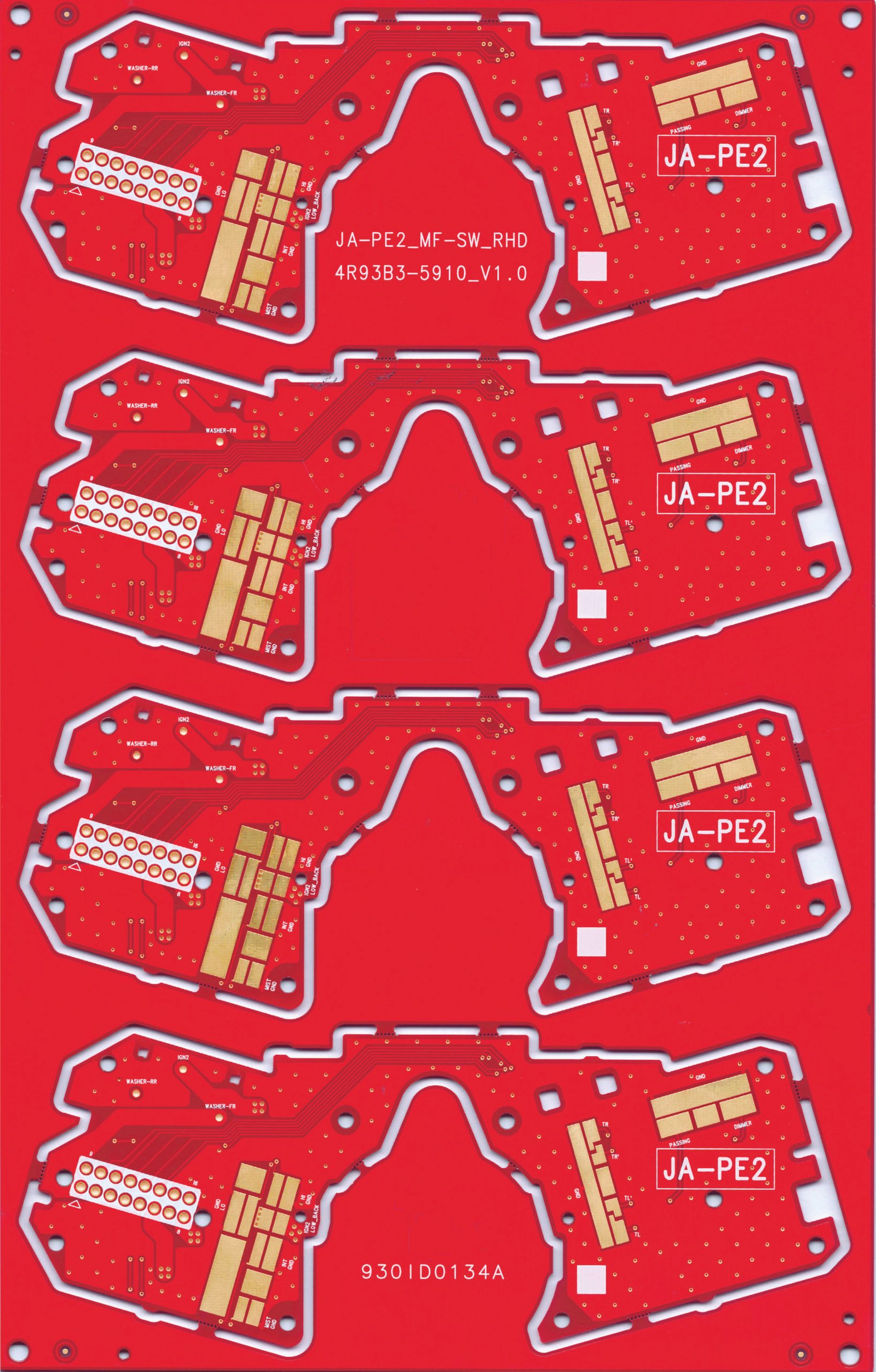
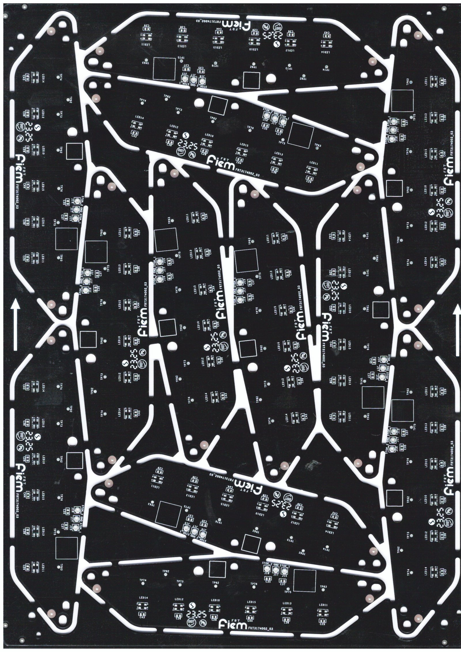
Double-Sided PCB are printed circuit boards with conductive layers on both the top and bottom sides, allowing for greater circuit density and complexity. They connect components using through-hole or surface-mount technology, with vias facilitating connections between layers.
Pros of Double Sided PCB
Increased Design Flexibility : Components can be placed on both sides of the board, allowing for more complex and compact circuit designs. Facilitates the use of more advanced circuitry, including mixed-signal circuits. Higher Circuit Density : With two conductive layers, more connections can be accommodated, leading to greater functionality in a smaller area. Cost-Effectiveness for Complex Designs : While more expensive than single-sided PCB, double-sided boards are significantly cheaper than multilayer boards for medium-complexity designs.They strike a balance between performance and cost. Improved Electrical Performance : Provides shorter and more direct electrical paths, reducing resistance and improving signal integrity.Enables better performance for high-speed circuits compared to single-sided PCB. Support for Advanced Applications : Essential for circuits requiring a moderate level of complexity, such as power supplies, amplifiers, and control systems. Widely used in industries like automotive, aerospace, and consumer electronics. Compact Size : Two layers allow for a more compact design, saving space and reducing the overall size of the device. Ideal for modern electronics where miniaturization is a key requirement. Ease of Prototyping and Testing : Easier to prototype and test compared to multilayer PCB, making them suitable for product development phases. Enhanced Heat Dissipation : Allows for better distribution of heat due to additional copper layers, improving thermal management. Increased Reliability : Reduces the risk of circuit failure as connections can be optimized for redundancy or reliability across the two layers.
Cons of Double Sided PCB
Higher Cost Compared to Single-Sided PCB : Double-sided PCB require additional processing steps, including plating through holes (PTH) and more complex soldering, which increases manufacturing costs.More expensive than single-sided boards, though still cheaper than multilayer PCB. Complex Design and Manufacturing : Designing circuits for two layers requires careful planning to avoid conflicts and ensure proper connectivity. Requires more sophisticated tools and expertise compared to single-sided boards. More Challenging Assembly : Components on both sides make assembly more intricate and time-consuming.
Increases the risk of errors during soldering or placement, especially for dense designs. Higher Risk of Short Circuits : The addition of vias and traces on both sides increases the chance of shorts or misalignments during manufacturing.Requires stringent quality control to prevent defects. Limited for Extremely Complex Designs : Double-sided PCB may not suffice for highly complex or dense circuits requiring more layers, such as advanced computing systems or large-scale industrial applications. Thermal Management Challenges : While double-sided PCB dissipate heat better than single-sided ones, they are less effective than multilayer PCB with dedicated thermal layers.May require additional components like heat sinks or thermal vias for high-power applications.
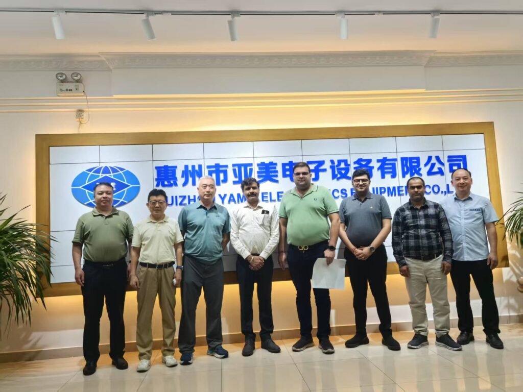
In a strategic move to strengthen our manufacturing capabilities and adopt cutting-edge technology, Team Signum recently completed a successful visit to China to explore and procure state-of-the-art equipment for our upcoming PCB production unit in Jammu.
The visit was part of our continuous commitment to innovation and excellence in the PCB industry. During the tour, our senior technical and operations team engaged with leading global manufacturers of PCB machinery and automation systems. The objective was to identify and integrate next-generation equipment that would enhance production efficiency, quality control, and scalability at our new facility.
Nov 11, 2024
Signum has successfully completed an audit with KIA Motors on 06-11-2024
May 28, 2025
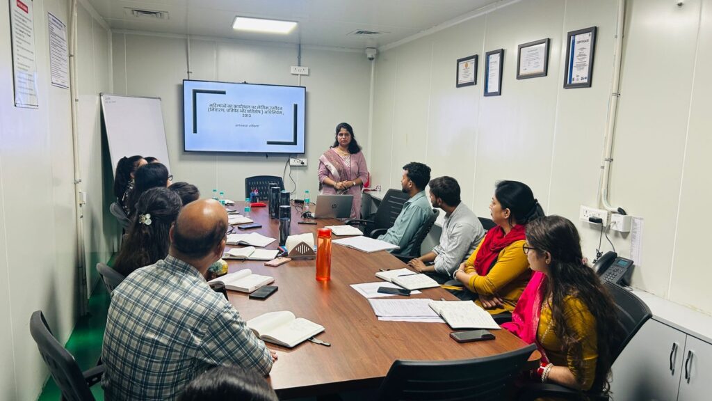
A POSH (Prevention of Sexual Harassment) training awareness session was successfully conducted at Signum by an external trainer, Ms. Malvika.
In a strategic move to strengthen our manufacturing capabilities and adopt cutting-edge technology, Team Signum recently completed a successful visit to China to explore and procure state-of-the-art equipment for our upcoming PCB production unit in Jammu.
The visit was part of our continuous commitment to innovation and excellence in the PCB industry. During the tour, our senior technical and operations team engaged with leading global manufacturers of PCB machinery and automation systems. The objective was to identify and integrate next-generation equipment that would enhance production efficiency, quality control, and scalability at our new facility.
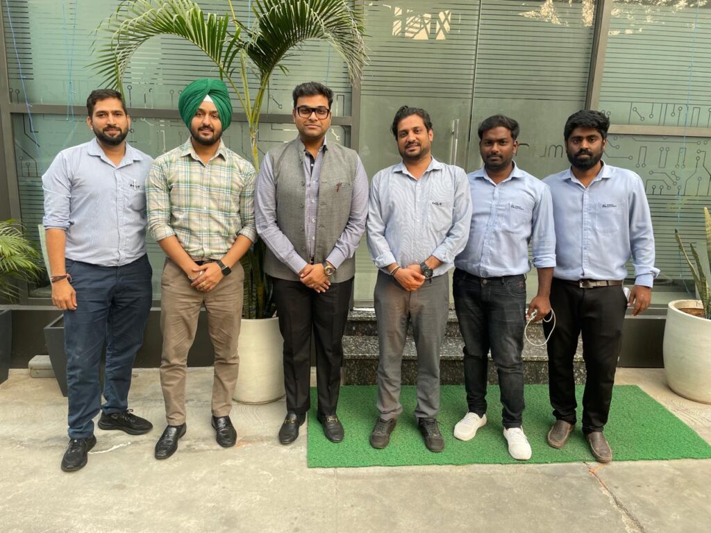
Team Signum Visits China to Upgrade Equipment for Advanced PCB Production at New Jammu Facility
In a strategic move to strengthen our manufacturing capabilities and adopt cutting-edge technology, Team Signum recently completed a successful visit to China to explore and procure state-of-the-art equipment for our upcoming PCB production unit in Jammu.
The visit was part of our continuous commitment to innovation and excellence in the PCB industry. During the tour, our senior technical and operations team engaged with leading global manufacturers of PCB machinery and automation systems. The objective was to identify and integrate next-generation equipment that would enhance production efficiency, quality control, and scalability at our new facility.