Sector Catered : Automotive, Lighting, Industrial Electronics, Home Appliances, Railways, Power Electronics, Automation, Storage Devices, Solar Systems.
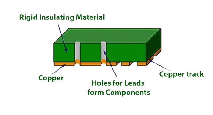
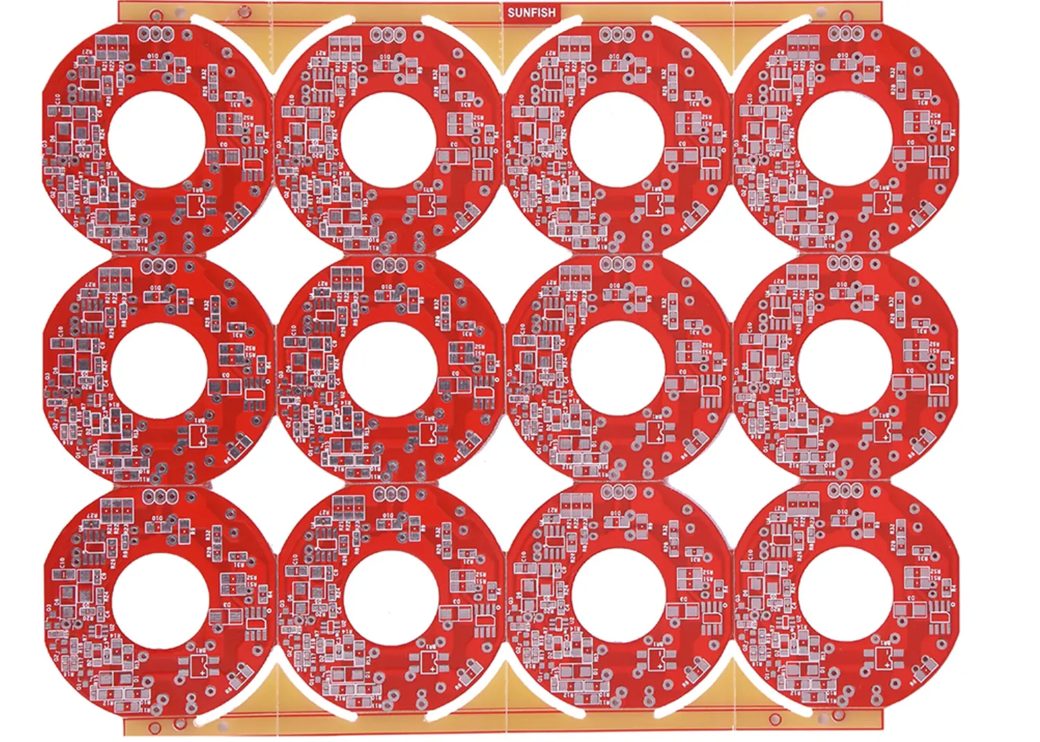
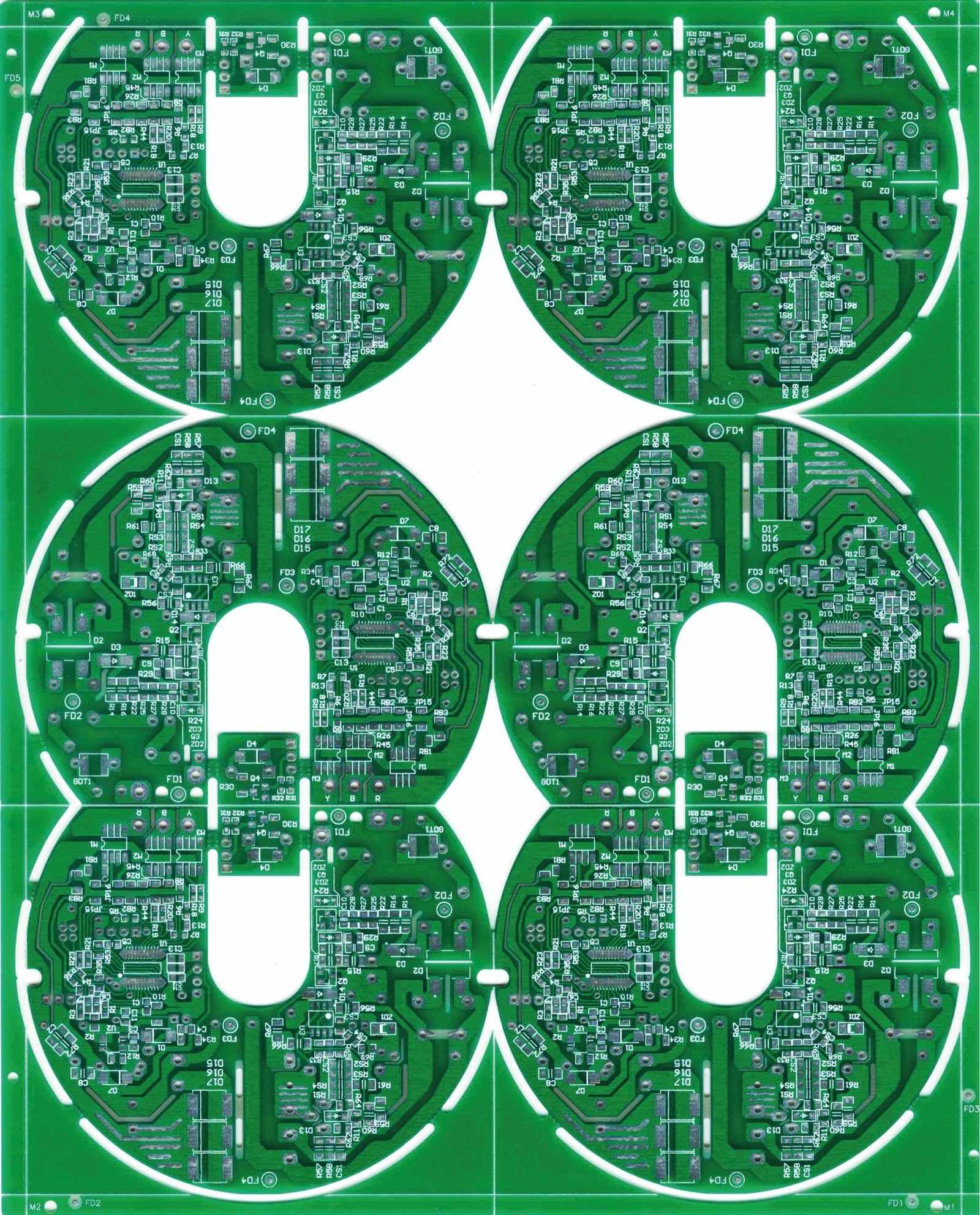
What is Single Sided PCB
Single-sided PCB (Printed Circuit Boards) are the simplest type of PCB, consisting of only one conductive layer of material (usually copper) on one side of the substrate.
Pros of Single Sided PCB
Cost-Effective : Lower Manufacturing Costs: Single-sided PCB are cheaper to produce due to their simple design and fewer manufacturing steps.Reduced Assembly Costs: Assembly is straightforward, often requiring only basic soldering techniques. Simple Design and Fabrication : Single-sided PCB are easier to design, especially for basic circuits.Fabrication processes are less complex, reducing production time and error rates. Easy Maintenance and Repair : With components and traces on separate sides, troubleshooting and repairing faults is easier.Ideal for prototyping and low-complexity applications. High Reliability for Simple Circuits : Fewer layers and connections mean a lower risk of electrical failure or signal interference.Well-suited for low-power and low-frequency applications. Quick Production : Simpler manufacturing processes allow for faster production cycles, making single-sided PCB ideal for rapid prototyping and mass production. Lightweight : Single-sided boards are lighter compared to double-sided or multilayer PCB, which is beneficial for portable or lightweight devices.
Cons of Single Sided PCB
Limited Circuit Complexity : Single-sided PCB allow components and traces only on one side, which restricts the complexity of the circuit.They are unsuitable for designs that require multiple interconnections or dense circuitry. Space Constraints : The lack of additional layers makes it challenging to design compact circuits for complex devices.The available space for routing traces is limited, increasing the risk of signal interference. Higher Signal Interference : With fewer routing options, traces may need to cross or run parallel to each other, leading to crosstalk and electromagnetic interference (EMI). Lower Durability : Single-sided PCB often use thinner copper layers, reducing durability and current-carrying capacity.They may not withstand harsh environments or high-power applications. Performance Limitations : Limited routing flexibility can lead to longer trace paths, increasing resistance and signal delay.They are not ideal for high-frequency or high-speed signal applications. Limited Scalability : Expanding or upgrading a single-sided PCB is difficult as additional layers cannot be added.Designers may need to transition to more advanced PCB like double-sided or multilayer for scalability.
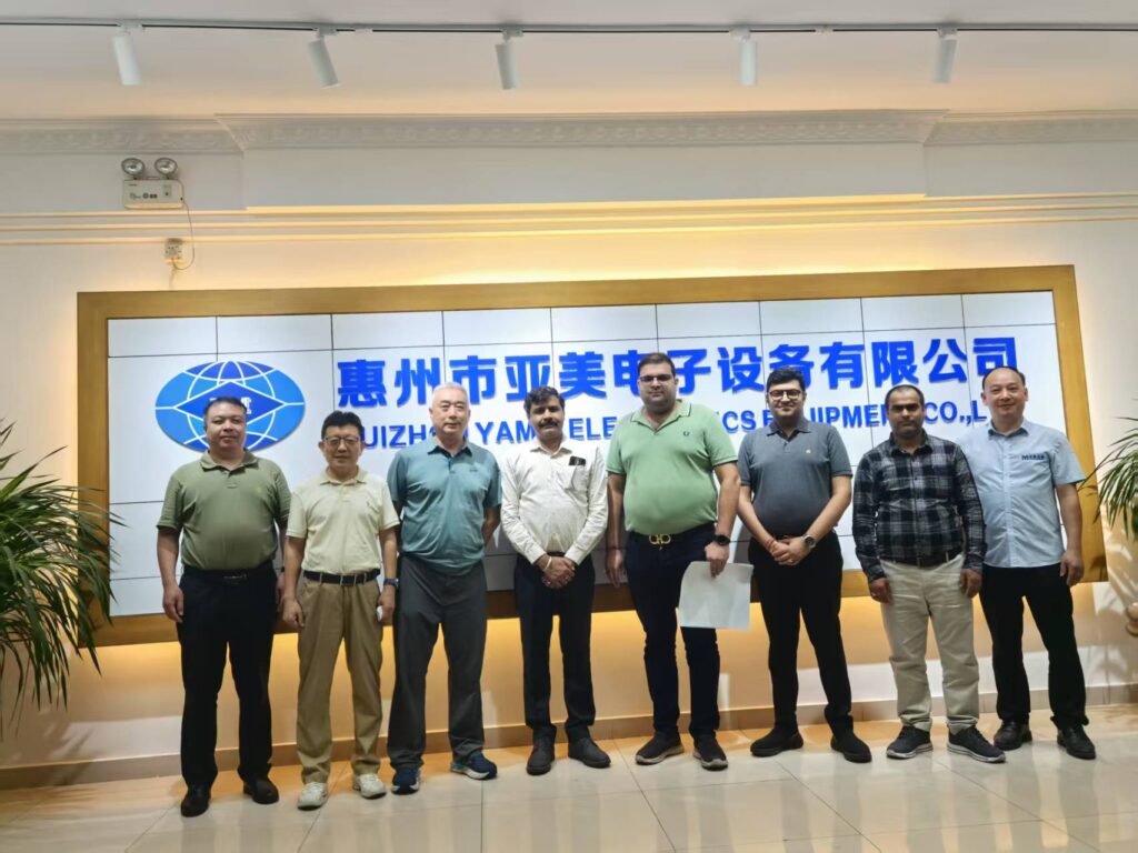
In a strategic move to strengthen our manufacturing capabilities and adopt cutting-edge technology, Team Signum recently completed a successful visit to China to explore and procure state-of-the-art equipment for our upcoming PCB production unit in Jammu.
The visit was part of our continuous commitment to innovation and excellence in the PCB industry. During the tour, our senior technical and operations team engaged with leading global manufacturers of PCB machinery and automation systems. The objective was to identify and integrate next-generation equipment that would enhance production efficiency, quality control, and scalability at our new facility.
Nov 11, 2024
Signum has successfully completed an audit with KIA Motors on 06-11-2024
May 28, 2025
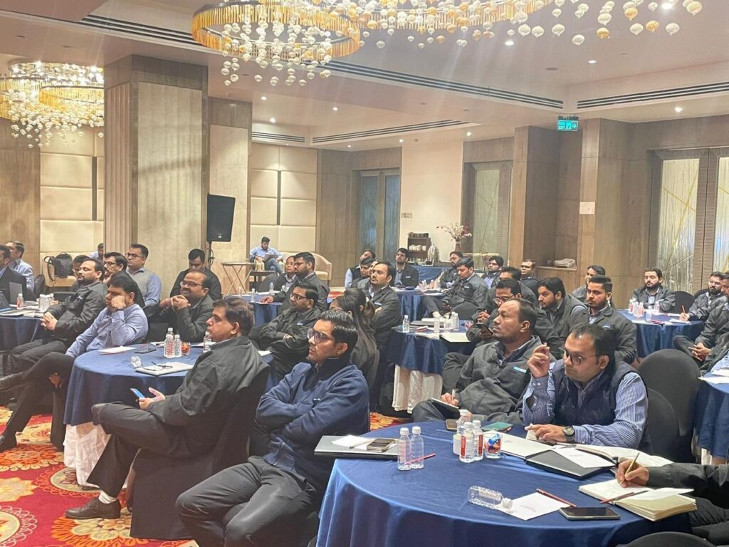
A POSH (Prevention of Sexual Harassment) training awareness session was successfully conducted at Signum by an external trainer, Ms. Malvika.
In a strategic move to strengthen our manufacturing capabilities and adopt cutting-edge technology, Team Signum recently completed a successful visit to China to explore and procure state-of-the-art equipment for our upcoming PCB production unit in Jammu.
The visit was part of our continuous commitment to innovation and excellence in the PCB industry. During the tour, our senior technical and operations team engaged with leading global manufacturers of PCB machinery and automation systems. The objective was to identify and integrate next-generation equipment that would enhance production efficiency, quality control, and scalability at our new facility.
Team Signum Visits China to Upgrade Equipment for Advanced PCB Production at New Jammu Facility
In a strategic move to strengthen our manufacturing capabilities and adopt cutting-edge technology, Team Signum recently completed a successful visit to China to explore and procure state-of-the-art equipment for our upcoming PCB production unit in Jammu.
The visit was part of our continuous commitment to innovation and excellence in the PCB industry. During the tour, our senior technical and operations team engaged with leading global manufacturers of PCB machinery and automation systems. The objective was to identify and integrate next-generation equipment that would enhance production efficiency, quality control, and scalability at our new facility.